| Issue |
Int. J. Metrol. Qual. Eng.
Volume 9, 2018
|
|
|---|---|---|
| Article Number | 13 | |
| Number of page(s) | 5 | |
| DOI | https://doi.org/10.1051/ijmqe/2018015 | |
| Published online | 20 November 2018 | |
Research Article
Evaluation of InGaAs/InP photodiode for high-speed operation at 4 K
1
University of South-Eastern Norway,
Borre, Norway
2
Justervesenet,
Kjeller, Norway
* Corresponding author: This email address is being protected from spambots. You need JavaScript enabled to view it.
Received:
11
December
2017
Accepted:
14
October
2018
Abstract
An optically controlled high-speed current source located at 4 K is likely to improve the performance of pulse-driven Josephson junction arrays. A custom photodiode module with an Albis PDCS24L InGaAs/InP PIN photodiode is investigated in order to determine the suitability at 4 K. The DC and frequency response were tested at room temperature and at temperatures down to 4 K. For continuous wave optical input, photocurrents above 15 mA were produced at both room temperature and 4 K. I–V measurements show that the threshold voltage increased from 0.5 V at room temperature to 0.8 V at 4 K. The transmission coefficient S21 of the optoelectronic system, including cables and modulated laser source, was measured using a vector network analyzer. Up to 14 GHz, the results showed that the frequency response at 4 K was not degraded compared to room temperature. At room temperature, reverse bias voltages of up to 3 V was required for the highest bandwidth, while at 4 K, the photodiode was operated at nearly full speed even at 0 V reverse bias.
Key words: optoelectronics / cryogenics / voltage standards
© E. Bardalen et al., published by EDP Sciences, 2018
 This is an Open Access article distributed under the terms of the Creative Commons Attribution License (http://creativecommons.org/licenses/by/4.0), which permits unrestricted use, distribution, and reproduction in any medium, provided the original work is properly cited.
1 Introduction
The pulse-driven Josephson Voltage Standard [1] is a technique for generating quantum-accurate voltages, by transferring short current pulses through Josephson junction arrays (JJA), which are often operated by cooling with liquid helium, at a temperature near 4 K. Any voltage waveform may be generated by modulating the repetition frequency f(t):
 (1)
where N is the number of Josephson junctions in series, h is Planck's constant and e is the electron charge. The Shapiro step number n depends on pulse parameters such as width and height [2].
(1)
where N is the number of Josephson junctions in series, h is Planck's constant and e is the electron charge. The Shapiro step number n depends on pulse parameters such as width and height [2].
Recently, very pure sine waves with voltages up to 1–2 V with frequencies up to a few kilohertz have been demonstrated using this technique [3,4]. Here, several Josephson junction arrays are operated in parallel, with the output voltage coupled in series, in order to increase the output voltage.
Utilizing optoelectronics to generate the high-speed pulses is believed to have several benefits compared to a direct electrical link between room-temperature pulse pattern generator (PPG) and the cryogenic chamber [5]. As the optical link is electrically isolated from the signal generator, reduced cable crosstalk and electromagnetic interference may be expected. By locating the photodiode close to the JJA, at 4 K in the cryogenic chamber, the cable length can be minimized and even eliminated.
The optoelectronic system consists of a laser source where the optical output is modulated by the PPG. The high-speed optical pulses are connected with an optical fiber to a photodiode, which converts the optical pulses into current pulses, which are transmitted to the JJA. The system may also contain other elements such as optical attenuators to fine-tune the pulse height.
In the following, an optoelectronic system has been set up for testing the small signal frequency response of a high-speed photodiode. However, the test setup does not include the JJA chip. The photodiode, a commercial InGaAs/InP PIN photodiode, is tested with the purpose of comparing the performance at 4 K compared to room temperature. Similar photodiodes have been shown to have no decrease in bandwidth at temperatures below 10 K, even operating with improved performance [6,7].
2 Test setup and sample preparation
A Rohde & Schwarz ZVL vector network analyzer (VNA) was used to measure the frequency response of the laser-photodiode setup. The output port of the VNA was connected to the modulation port of a modulator-integrated 1310 nm Eudyna FLD3F10NP-A DFB laser, which is specified to have a minimum bandwidth of 10 GHz and maximum optical output power of around 1 mW. The laser was also biased with a constant DC current. The optical output consisted of a continuous wave (CW) combined with a smaller modulated signal as the output power from the VNA is not sufficient to completely extinguish the CW.
In addition, a higher powered 1310 nm laser source, with optical output power up to 30 mW, was used to measure the photocurrent for different CW powers.
The optical output from the laser was coupled via a single mode optical fiber (SMF) to the photodiode. The electrical output from the photodiode was connected to a coaxial cable. A bias tee separated the RF output to the input port of the VNA and the DC component to a Keithley 6430 source meter, which was also used to apply bias voltage to the photodiode.
The photodiode used in these tests were Albis PDCS24L photodiodes mounted on small ceramic submounts. These photodiodes were selected as they have a bandwidth of up to 28 Gbps and are available as bare chips, thus enabling custom packaging for later integration with the Josephson system. Different configurations of illumination and sample mounting were tested to uncover potential limitations in photodiode packaging. The photodiode is illuminated via an integrated lens, which makes optical alignment rather easy. The sample configurations were as follows:
2.1 Sample 1: Photodiode with direct optical fiber coupling
In the first configuration, optical fiber-connected samples were made for directly immersing in liquid helium. The photodiodes were adhesively bonded to a 2 mm thick Rogers RO4350b sample holder with copper coplanar waveguide (CPW) transmission lines designed for 50 Ω characteristic impedance. The ceramic submount was glued directly to the sample holder and wire-bonded to the CPW. Surface-mounted SMP connectors were soldered to the CPW, where a high-speed coaxial cable was connected, as shown in Figure 1.
A single mode fiber terminated by glass ferrule (Thorlabs part no: SMPF021) was inserted into a matching borosilicate sleeve (Thorlabs part no: 51-2800-1800) that was aligned to the photodiode and glued directly to the sample holder with epoxy (Master Bond EP29LPSPAO-1 BLACK).
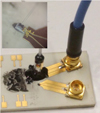 |
Fig. 1 Sample 1. Assembly with adhesively bonded fiber components and SMP connector. Inset shows microscope image of photodiode on submount with wire bonds, with a manually aligned optical fiber. |
2.1 Sample 2: Photodiode mounted in cryoprobe
The second sample was mounted inside a cryogenic probe station, Lakeshore CPX, for operation at temperature between 4 K and room temperature in vacuum. The ceramic submount was glued to a small alumina plate that was thermally anchored to the cold plate of the cryoprobe.
A biconvex lens mounted to a micrometer stage was used to focus the beam from the SMF fiber through the outer cryoprobe window, as seen in Figure 2. The inner cryoprobe window was removed as it blocks infrared radiation. An RF probe was used to measure the signal output from the photodiode.
Additionally, for comparison with sample 1 and 2, a commercial photodiode module, Albis PQW20A, was tested in the same setup. This module also contains an Albis InGaAs PIN photodiode but has an integrated biasing circuit that includes a 50 Ω resistor to ground. This resistor is likely intended to minimize standing waves in the electrical output cable. In this case, the bias voltage is applied directly to the PQW20A module.
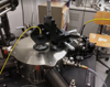 |
Fig. 2 Sample 2. The photodiode is located in vacuum and is illuminated using a focused beam through cryoprobe window. |
3 Results
Sample 1 was measured at room temperature and in liquid helium, while for sample 2, S21 was measured at temperatures 20, 100, and 200 K as well as at room temperature.
The transmission coefficient S21 was measured from frequencies between 100 kHz and 14 GHz for various bias voltages of the photodiode.
3.1 Effects of optical fiber alignment and cable length
The measured transmission coefficients include attenuation and reflections inside the complete system, including the laser, photodiode and in cables/connectors. To evaluate the effect of these different factors, the photodiode was first measured at room temperature with the optical fiber aligned by a micrometer stage. Next, the optical fiber was permanently mounted and the assembly was tested with different cable lengths in order to establish a baseline for the cryogenic measurements. Figure 3shows S21 from frequencies 100 kHz to 14 GHz. At frequencies higher than 5 GHz, the permanent fiber alignment slightly reduced the transmission by about 2 dB, compared to the manual alignment. Inserting a 2 m coaxial patch cable between the bias tee and the SMP connector further reduced S21, in particular at frequencies above 1 GHz.
Sample 2 has a similar response to sample 1. However, due to the less efficient optical coupling, the frequency response was reduced by 6–8 dB.
Both sample 1 and sample 2 contained large oscillations in the frequency response, of around 1–4 dB with a period of around 125 MHz.
The overall transmission for the PQW20A module was reduced by more than 3 dB for all frequencies compared to sample 1. This is consistent with the use of the 50 Ω resistor, which theoretically reduces the power output to the output connector by half. The large oscillations seen in sample 1 and 2 were reduced significantly, although they are still present.
The overall system response was less than −30 dB for all frequencies, which can mostly be attributed to a high loss in the laser modulation input. In the best case, a −3 dB bandwidth of the system can be found at approximately 10 GHz. However, packaging and coaxial cables reduced the bandwidth significantly.
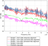 |
Fig. 3 Transmission for sample 1, sample 2 and the Albis PQW20A module in different configurations at room temperature. Reverse bias voltage of 3 V is used in all measurements. |
3.2 Temperature effects
The 2 m patch cable is used following the results in order to facilitate immersion in the liquid helium Dewar. A numerical smoothing function was applied to all results in order to improve the readability of the curves.
The DC response of the photodiode in dark condition is shown in Figure 4. It can be seen that the threshold voltage increases, as expected, at lower temperatures.
The photocurrent response to CW input for different laser currents was measured at room temperature and at 4 K for sample 1, as shown in Figure 5. The photodiode was able to produce currents well above 15 mA at both temperatures. At 4 K, the current response was reduced to by approximately 10% compared to the room temperature result.
Figure 6shows the frequency response at room temperature and at 4 K for sample 1 for reverse voltages between 0 and 3 V. At room temperature, the frequency response was maximized at bias voltages of approximately 3 V. At 4 K, full speed was achieved at very low bias voltage. Changing the bias voltage from 0 to 3 V resulted in less than 1 dB difference in S21. The responsivity was reduced by around 1.5 dB at 4 K compared to room temperature.
For comparison, the measurements were repeated in the cryoprobe for sample 2, using a focused beam as described in Section 2. The sample stage reached a temperature of 4 K, while the temperature of the cryogenic probe arm was 20 K. Therefore, the temperature is assumed to be 20 K. Figure 7 shows that at 20 K, the transmission curves overlap the curves for room temperature. Furthermore, the measurements show a lower dependence on bias voltage at both temperatures. At 20 K, the gain effect of increasing bias voltage from 0 to 3V is less than 1 dB.
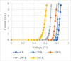 |
Fig. 4 I–V measurements of sample 1 (4 K) and sample 2 (20, 100, 200 and 296 K). |
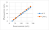 |
Fig. 5 Photocurrent generated by sample 1 for varying laser current, with 0 V bias applied to photodiode. |
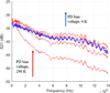 |
Fig. 6 Transmission measurements of sample 1 at room temperature (red lines) and at 4 K in liquid helium (blue lines) for different bias voltages (0, 1, 2, 3 V). A numerical smoothing function was used to remove oscillations seen in Figure 3. At room temperature, full speed is reached for bias voltages close to 3 V. At 4 K, the photodiode reaches full speed at a bias voltage close to 1 V. |
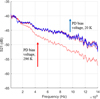 |
Fig. 7 Transmission measurements of sample 2. Transmission S21 at room temperature (red lines) and 20 K in cryoprobe (blue lines) for different bias voltages (0, 1, 2, 3 V). A numerical smoothing function was used to remove oscillations seen in Figure 3. At room temperature, increasing the reverse voltage above 2 V has almost no influence on bandwidth, while at 20 K, 0.5 V is sufficient. |
4 Discussion
The photodiode frequency performance at low temperatures is affected by several temperature-dependent effects. These include incomplete ionization and changes in physical properties such as bandgap and electrical mobility. The reduced need for bias voltage at 4 K may be explained by a higher electric field in the absorption layer of the photodiode due to the increase in bandgap and changes in the Fermi level, as well as changes in electrical mobility in InGaAs and InP. The reduced DC responsivity, as shown in Figure 5, observed at 4 K for sample 1, may be partly explained by increased bandgap in InGaAs. However, thermal deformations may also have influenced the optical coupling efficiency between the photodiode and the optical fiber. This may also explain the lower overall frequency response at 4 K for sample 1.
Operation of JJA would require current pulse amplitudes comparable to the critical current density Ic in the JJA [2], which may be up to several mA. At higher optical power input, the frequency response may be reduced due to space-charge effects [8] and changes in bias voltage caused by the load resistance [9]. For JJAs, it is common to terminate the array with a 50 Ω resistor. Thus, higher reverse bias may be needed at 4 K than the results shown here indicate.
5 Conclusions and further work
A setup consisting of a modulated laser and a commercial InGaAs/InP photodiode was characterized at room temperature and 4 K using a network analyzer. The results show that the cryogenic environment does not negatively impact the photodiode response, and may even improve performance as lower bias voltage is required.
This may enable the operation of Josephson arrays using optical fiber-coupled photodiodes cooled to 4 K. However, further consideration of impedance matching and transmission line design may be necessary to reduce unwanted reflections.
The photodiode response to optical pulses with amplitudes of several mW must be tested using a high-speed PPG, suitable laser source/modulator and oscilloscope.
The prospect of closely integrating the photodiode with the Josephson array is to be investigated. For example, photodiodes may be flip-chip bonded to a silicon substrate with superconducting transmission lines, or directly onto the JJA-integrated circuit silicon chip.
Another interesting prospect is to perform numerical simulations of both photodiode behavior and the complete system behavior. Such simulations may enable better predictions of performance, also enabling improvement in system design.
Acknowledgments
This work was partly carried out with funding by the European Union within the EMRP JRP SIB59 Q-WAVE and EMPIR JRP 15SIB04 QuADC. The EMRP and EMPIR are jointly funded by the EMRP participating countries within EURAMET and the European Union.
In addition, the work was also partly funded by a PhD scholarship from University College of Southeast Norway, funded by the Norwegian Ministry of Education and Research.
References
- S.P. Benz, C.A. Hamilton, A pulse-driven programmable Josephson voltage standard, Appl. Phys. Lett. 68, 3171–3173 (1996) [Google Scholar]
- J.M. Williams, T.J.B.M. Janssen, L. Palafox, D. A. Humphreys, R. Behr, J. Kohlmann et al., The simulation and measurement of the response of Josephson junctions to optoelectronically generated short pulses, Supercond. Sci. Technol. 17, 815–818 (2004) [Google Scholar]
- N.E. Flowers-Jacobs, A.E. Fox, P.D. Dresselhaus, R.E. Schwall, S.P. Benz, Two-volt Josephson arbitrary waveform synthesizer using Wilkinson dividers, IEEE Trans. Appl. Supercond. 26 (2016), doi: 10.1109/TASC.2016.2532798 [Google Scholar]
- O.F. Kieler, R. Behr, R. Wendisch, S. Bauer, L. Palafox, J. Kohlmann, Towards a 1 V Josephson arbitrary waveform synthesizer, IEEE Trans. Appl. Supercond. 25, 1–5 (2015) [Google Scholar]
- J. Gran, H. Malmbekk, K. Lind, Photodiodes as current source in high-frequency low temperature applications, in 2014 Conference on Precision Electromagnetic Measurements (CPEM 2014), 2014, pp. 266–267 [Google Scholar]
- L.A. Bunz, E.K. Track, S.V. Rylov, F.-Y. Perng, J.D. Morse, Fiber optic input and output for superconducting circuits, Proc. SPIE 229–236 (1994) [Google Scholar]
- Y.M. Zhang, V. Borzenets, N. Dubash, T. Reynolds, Y.G. Wey, J. Bowers, Cryogenic performance of a high-speed GaInAs/InP p–i–n photodiode, J. Lightw. Technol. 15, 529–533 (1997) [CrossRef] [Google Scholar]
- K.J. Williams, R.D. Esman, M. Dagenais, Effects of high space-charge fields on the response of microwave photodetectors, IEEE Photon. Technol. Lett. 6, 639–641 (1994) [CrossRef] [Google Scholar]
- P.S. Matavulj, D. Gvozdić, J. Radunović, J.M. Elazar, Nonlinear pulse response of pin photodiode caused by the change of the bias voltage, Int. J. Infrared Millimeter Waves 17, 1519–1528 (1996) [Google Scholar]
Cite this article as: Eivind Bardalen, Bjørnar Karlsen, Helge Malmbekk, Muhammed Nadeem Akram, Per Ohlckers, Evaluation of InGaAs/InP photodiode for high-speed operation at 4 K, Int. J. Metrol. Qual. Eng. 9, 13 (2018)
All Figures
|
Fig. 1 Sample 1. Assembly with adhesively bonded fiber components and SMP connector. Inset shows microscope image of photodiode on submount with wire bonds, with a manually aligned optical fiber. |
| In the text | |
|
Fig. 2 Sample 2. The photodiode is located in vacuum and is illuminated using a focused beam through cryoprobe window. |
| In the text | |
|
Fig. 3 Transmission for sample 1, sample 2 and the Albis PQW20A module in different configurations at room temperature. Reverse bias voltage of 3 V is used in all measurements. |
| In the text | |
|
Fig. 4 I–V measurements of sample 1 (4 K) and sample 2 (20, 100, 200 and 296 K). |
| In the text | |
|
Fig. 5 Photocurrent generated by sample 1 for varying laser current, with 0 V bias applied to photodiode. |
| In the text | |
|
Fig. 6 Transmission measurements of sample 1 at room temperature (red lines) and at 4 K in liquid helium (blue lines) for different bias voltages (0, 1, 2, 3 V). A numerical smoothing function was used to remove oscillations seen in Figure 3. At room temperature, full speed is reached for bias voltages close to 3 V. At 4 K, the photodiode reaches full speed at a bias voltage close to 1 V. |
| In the text | |
|
Fig. 7 Transmission measurements of sample 2. Transmission S21 at room temperature (red lines) and 20 K in cryoprobe (blue lines) for different bias voltages (0, 1, 2, 3 V). A numerical smoothing function was used to remove oscillations seen in Figure 3. At room temperature, increasing the reverse voltage above 2 V has almost no influence on bandwidth, while at 20 K, 0.5 V is sufficient. |
| In the text | |
Current usage metrics show cumulative count of Article Views (full-text article views including HTML views, PDF and ePub downloads, according to the available data) and Abstracts Views on Vision4Press platform.
Data correspond to usage on the plateform after 2015. The current usage metrics is available 48-96 hours after online publication and is updated daily on week days.
Initial download of the metrics may take a while.